PCB Capability
|
Material
|
FR4, High TG FR4, Aluminum, Ceramic, PI, PET
|
|
Layer
|
1-32 layers
|
|
Board thickness
|
0.6mm-8.5mm
|
|
Copper thickness
|
0.5oz – 6oz
|
|
Board thickness Tolerance
|
+/- 10%
|
|
Min Line Width
|
0.1mm(4mil)
|
|
Min Line Space
|
0.1mm(4mil)
|
|
Min Hole Size
|
0.1mm(4mil)
|
|
Solder mask
|
Green, black, Blue, White, Yellow, Red, etc
|
|
Silkscreen
|
White, Yellow, Red, Black, etc
|
|
Surface finish
|
HASL, Immersion Gold, OSP, Immersion Silver, Electrolytic gold
|
|
More info or other requirements you need, please feel free to contact us!
|
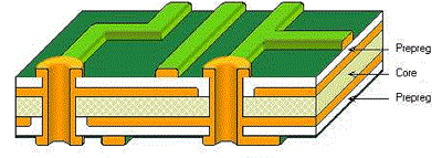
PCB Manufacturing Process
PCB manufacturing process is different for different PCB factories, different layers of PCB, but some steps are same and all of them will have to do. Single layer PCB and Double layers PCB are all use the raw material so that they don't need to do Lamination process, they are easy to do. So here we will show 4 layers PCB manufacturing process as multilayer PCB.
4 Layers PCB Manufacturing Process
Usually we fabricate 4 layers PCB as the following steps, and we will show the manufacturing process as this 4 layers PCB. But here won't all the step just show some important step which can help you to know how we manufacture PCB, because it will make you lost if we list all the steps. But don't hesitate to contact if you need more information, we are always here for you.
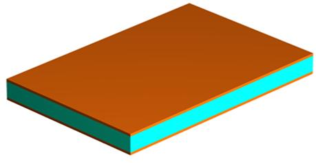
1. Cutting Sheet
We have to cut a small size board from the big raw material, assume we will manufacture a PCB with the size 10 mm * 10 mm. As the following picture, you will find the raw material include two copper layers that will be final layer 2 and layer 3, and both are inner layer.
2. Chemical Clean
To get good quality of the etched pattern, and make sure the combination between corrosion resistant layer and substrate surface is strong, so the substrate surface must be without oxidation layer, oil, dirt, fingerprints, and other contaminants. So we need to do chemical clean.
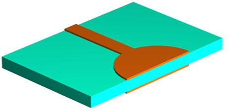
3. Inner Layers
Circuit layer is a complex process, including Dry Film Lamination, Expose, Develop and Copper etching.
4. Lamination
After inner layers, we will laminate so that we can get a 4 layers structure from 2 layers structure
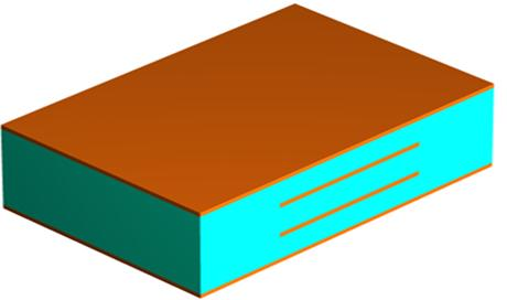
5. CNC Drilling
6. Plated Through Hole
After lamination and drilling, we get a 4 layers structure, but we need to do plated through holes to connect different layers.
7. Outer Layer
After plated through holes we will do outer layer now like inner layers, but you will find we do Tin Pattern Electro Plating to protect copper layers, but will strip Tin after Copper Etch.

8. Soldermask
Soldermask is used to protect the copper layers meanwhile avoid short circuit when SMT and weld.
9. Surface Finishing
PCB surface finishing includes HASL, OSP, ENIG and so on, which is protect pads and prolongs the self left, because it may take long time before we do SMT or weld .
10. Outline
After soldermask and surface finishing, at last we need V-Cut or Routing to make the final outline meet PCB files.
11. FQC, Packaging and Shipping
After outline, we will check the final PCB quality, package and ship to customers.
Now you may know how to fabricate PCB in our workshop, meanwhile we also welcome you to our factory to see more details, and please let us know if you would like to order PCB, KLS will be your best choice.
|