|
|
||||||||||||||
|
| Home > Solutions > PCB Assembly | ||||||||||||||||||
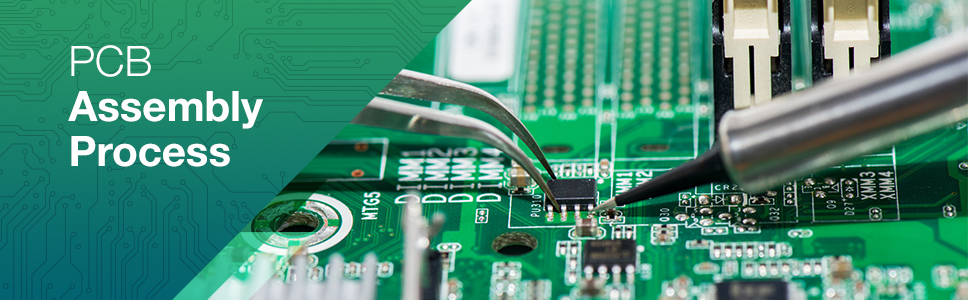
PCB Assembly
KLS Company is keen on being your partner in PCB Assembly outsourcing and Production. We have over 10 years experience in PCB Assembly both as high volume PCB Assembly outsourcing partners as well as catering to R&D driven developments and prototype development and support. To us as a company no project is too big to fulfill the demands of an outsourced production line partner, nor too small as a facilitator in state of the art emerging technology development with regard to PCB Assembly. We strive to accommodate, adapt, improve and revolutionize the process of printed circuit board assembly with the resources of our facilities and highly trained professional staff.
PCB Assembly Capabilities:
PCB Assembly and Production Process Within a printed circuit board electronics assembly / production or manufacturing process there are a number of individual stages. However it is necessary for them all to work together to form an integrated overall process. Each stage of assembly and production must be compatible with the next, and there must be feedback from the output to the input to ensure that the highest quality is maintained. In this way any problems are detected quickly and the process can be adjusted accordingly.
The solder paste is a paste of small grains of solder mixed with flux. This can be deposited into place in a process that is very similar to some printing processes. Using the solder screen, placed directly onto the board and registered in the correct position , a runner is moved across the screen squeezing a small mount of solder paste through the holes in the screen and onto the board. As the solder screen has been generated from the printed circuit board files, it has holes on the positions of the solder pads, and in this way solder is deposited only on the solder pads. The amount of solder that is deposited must be controlled to ensure the resulting joints have the right amount of solder.
The components placed onto the board are held in place by the tension of the solder paste. This is sufficient to keep them in place provided that the board is not jolted. In some assembly processes, the pick and place machines add small dots of glue to secure the components to the board. However this is normally done only if the board is to be wave soldered. The disadvantage of the process is that any repair is made far more difficult by the presence of the glue, although some glues are designed to degrade during the soldering process. The position and component information required to be programmed the pick and place machine is derived from the printed circuit board design information. This enables the pick and place programming to be considerably simplified.
b. X-ray Inspection: checks for BGAs, QFN and bare circuit boards. c. AOI Testing: checks for solder paste, 0201 components, missing components and polarity. d. ICT (In-Circuit Test). e. Functional test (Following your test procedures).
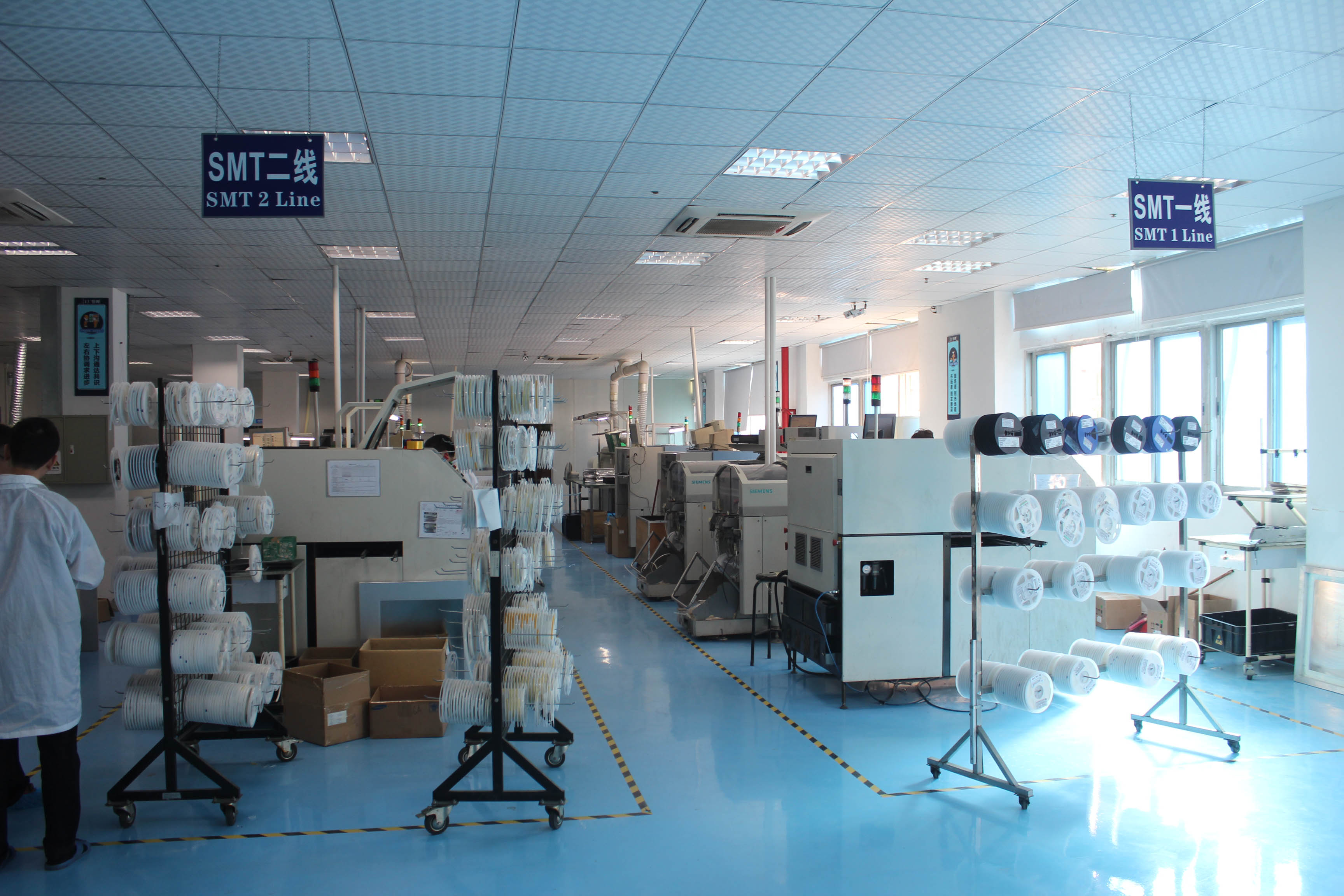
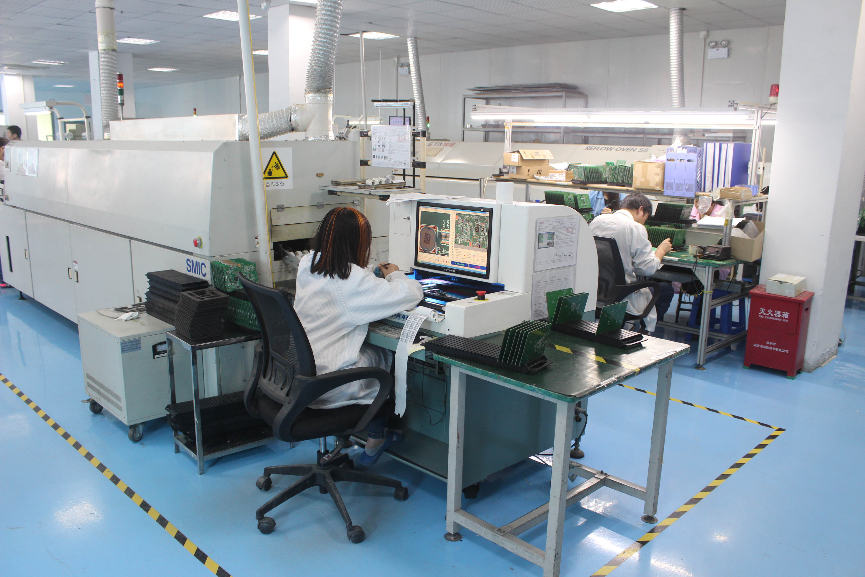
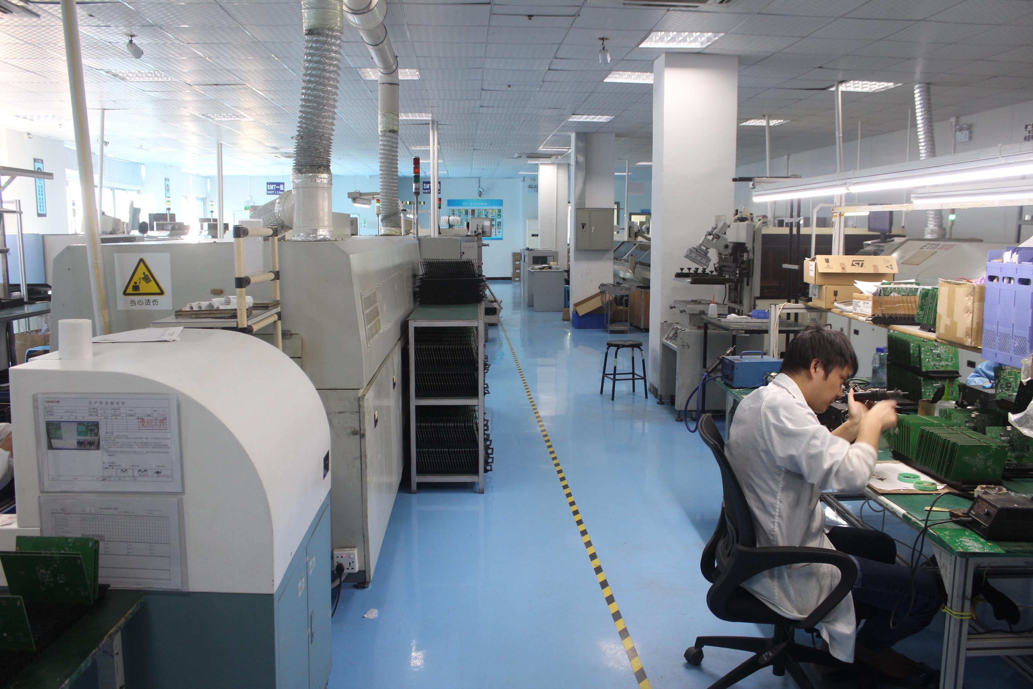
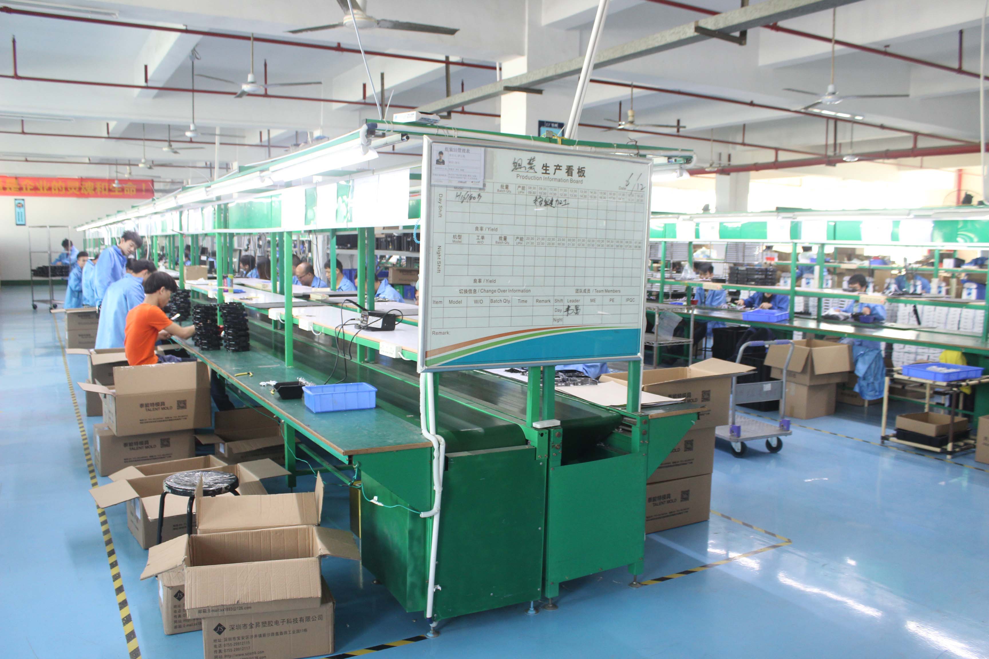
SMT & THT Line, Assembly Line
|
|
||||||||||||||||||||||||||||||||||||||||||||||||||||||||||||||
Kinglisheng(Shenzhen) Electronics & Techonoloy Co., Limited (C) 2015 All rights reserved
Mobile telephone:13266599929 MarK Email:mark@jlspcba.com Web:www.jlspcba.com
Address:No.634 Sha Jing road, Bu Yong, Shajing street Baoan district, Shenzhen city, China
|